I use the global human network,
provide with the information and proposals in which semiconductor technology / industry is overviewed.
I use my experience on semiconductor technology and its industry obtained at TOSHIBA CORPORATION and Tohoku University, and activate the global human network with academia and the global companies I had gained when I worked in the US and I was engaged in IEEE Committee Asian Arrangement Chair. This allows me to offer the detailed information in which semiconductor industry / technology is overviewed, and to make proposals on semiconductor business strategy.
I hear that my maternal grandfather, Toshio Matsushita, was Deputy General Manager of Nagahama Plant before World War II (current Shiga Plant Nagahama Area of Mitsubishi Chemical Corporation), and he was also General Manager who had contributed to launch of petrochemical in the dawn at the laboratory of Keihin area (current Tsurumi Plant of Mitsubishi Chemical Corporation).
Because of that, my mother's house had a beaker, flask, alcohol lamp, graduated cylinder, and they formed a treasure mountain for me, an elementary school boy. That makes me strongly want to contribute to the MCG Group as much as I can. I feel as if my grandfather stood and gave me an instruction like this or that. (haha)
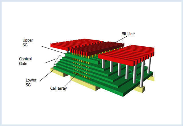
I used to lead research and development on all the semiconductor memories,
including the invention of 3DNAND Flash forming 10 trillion yen market, that was nurtured in forefront.
I believe what our clients expect me to do is to offer the latest trends of semiconductor market / technology, make proposals and give support for semiconductor business strategy, and help them develop new businesses through the fore-mentioned.
To collect the updated information, I make arrangement for the technology exchange meeting with responsible staff of device makers, and gain trust through my human network to directly hear users' issues and real intention about materials. I get back to my clients with the feedback gained by the fore-mentioned procedure.
When it comes to semiconductor technology, I used to work on advanced memory research and development at TOSHIBA CORPORATION for 31 years, and took the lead on research and development for all the semiconductor memories including DRAM, Flash, MRAM, FeRAM, SOI. I use my experience and knowledges that can respond to the general semiconductor technology such as advanced logic, advanced memory, power device, CMOS Image Sensor, quantum technology, to maximum level.
As for the research performance results, I give the information on semiconductor related technology and the market, proposals for new businesses and individual consultations to the MCG Group. In addition to that, I did research on trends for non-von Neumann type computing and quantum technology in 2017, research for storage class memory technology in 2018, research for patent application technology trends on GaN*3 power device, research for building of intellectual property portfolio (gallium oxide device), in the technology market trend research such as NEDO*1, Patent Office, NICT*2. and they have brought a favorable evaluation to me.
I hope that I will conduct technology trend research on semiconductor and the peripheral fields and make proposals for business strategy, in order to use the earned experience and knowledge to offer the information with higher quality.
- NEDO: New Energy and Industrial Technology Development Organization
- NICT: National Institute of Information and Communications Technology
- GaN: Gallium Nitride